Researchers grow 2-inch single-crystal graphene with 2 to 5 layers on oxidized copper wafers
A CVD method on Cu(111)–Cu2O(111) gives layer-controlled graphene and patterned Bernal and rhombohedral stacking in trilayers, a laboratory-scale result.
Researchers have reported a chemical vapor deposition method for growing layer-controlled graphene on oxidized single-crystal copper wafers, according to a paper in Advanced Materials. The substrate is atomically flat and combines Cu(111) with Cu2O(111) as a heterogeneous catalytic surface. wiley.com
Advanced Materialswiley.comOpen source ↗
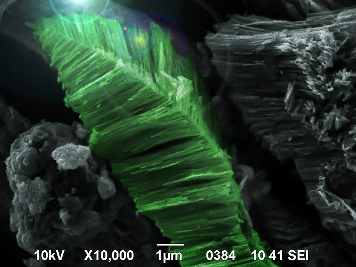
Using this substrate, the authors obtained 2-inch single-crystalline graphene films with the number of layers tuned from 2 to 5. The approach is described as synchronous and unidirectional epitaxy.
By engineering the atomic steps of high-index Cu surfaces, the team created a deterministic spatial pattern of alternating Bernal and rhombohedral stacking in trilayer graphene. The stacking was confirmed by near-field nano-optics and angle-resolved photoemission spectroscopy.
According to the authors, the wafer-scale films show uniform thickness, high crystallinity and an ultra-flat surface. They state that the framework addresses layer control, wafer-scale single crystallinity and stacking-order modulation together, and provides a material basis for further device studies. wiley.com
Advanced Materialswiley.comOpen source ↗