Fraunhofer IZM makes wafer-scale 3D energy-filter diode demonstrator for neutrino mass experiments
Fraunhofer IZM and the University of Münster made a silicon diode with 250-micrometer hexagonal pits that separates electrons by angle; simulations indicate 3–5x less background.
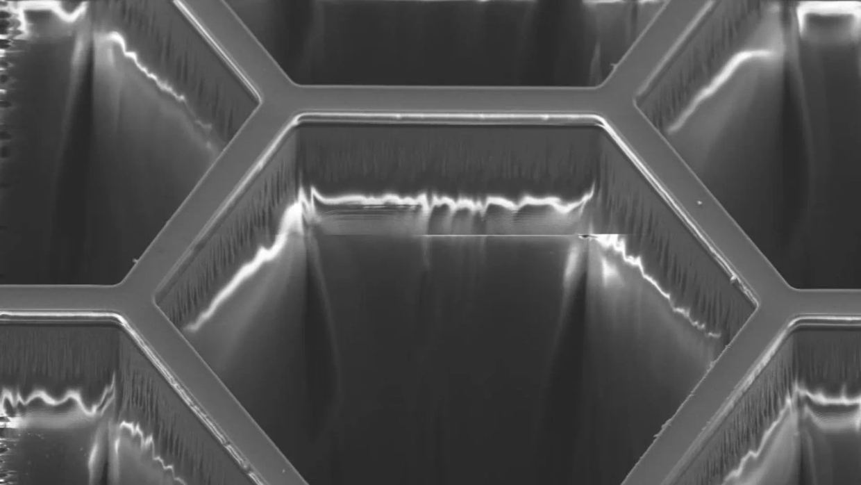
Researchers at Fraunhofer IZM and the University of Münster have developed a wafer-scale manufacturing process for a "3D energy-filter diode", Interesting Engineering reports. The silicon device carries a honeycomb pattern of pits 250 micrometers deep. It is designed to distinguish signal electrons from background electrons by their angle of incidence interestingengineering.com
Interesting Engineeringinterestingengineering.comOpen source ↗. The diode remains a demonstrator, not a detector ready for use
interestingengineering.com
Interesting Engineeringinterestingengineering.comOpen source ↗.
Why the angle of incidence matters
The device measures a particle's energy and the angle at which it hits the detector. In experiments such as KATRIN (the Karlsruhe Tritium Neutrino Experiment), scientists study the fine energy spectrum of tritium beta decay to determine the neutrino mass interestingengineering.com
Interesting Engineeringinterestingengineering.comOpen source ↗. The measurement is affected by background: "imposter" electrons reach the detector with almost the same kinetic energy as signal electrons
interestingengineering.com
Interesting Engineeringinterestingengineering.comOpen source ↗.
The two groups differ in geometry. Background electrons typically arrive at shallow angles below ten degrees, while signal electrons enter at angles up to 50 degrees interestingengineering.com
Interesting Engineeringinterestingengineering.comOpen source ↗. Conventional detectors operating in strong magnetic fields and ultrahigh vacuum cannot resolve this difference
interestingengineering.com
Interesting Engineeringinterestingengineering.comOpen source ↗.
In the new Si-PIN diode, wide-angle signal electrons hit the active sidewalls of the hexagonal pits and produce a signal. Shallow-angle background electrons pass through to the inactive floor of the pit interestingengineering.com
Interesting Engineeringinterestingengineering.comOpen source ↗. Computer simulations indicate that this architecture could reduce background by a factor of three to five
interestingengineering.com
Interesting Engineeringinterestingengineering.comOpen source ↗.
Manufacturing steps
The first detector wafers had a 24-sided geometry that did not fit standard 200-millimeter cleanroom tools. Engineers at Fraunhofer IZM temporarily wax-bonded the custom wafers onto standard 200 mm carrier plates interestingengineering.com
Interesting Engineeringinterestingengineering.comOpen source ↗.
The deep, near-vertical trenches were etched by Deep Reactive Ion Etching (DRIE). The team adjusted process pressure, plasma power and wafer temperature to eliminate structural flaws known as "silicon grass" interestingengineering.com
Interesting Engineeringinterestingengineering.comOpen source ↗.
The last step was passivation of the 250-micrometer sidewalls. Standard thermal oxidation would have destroyed the metal layers already on the diode, so the team used plasma-enhanced chemical vapor deposition (PECVD) at 175 degrees Celsius. It coated the upper, middle and lower sidewalls with insulating silicon dioxide to suppress dark currents interestingengineering.com
Interesting Engineeringinterestingengineering.comOpen source ↗.
The new wafers are now undergoing test measurements at the University of Münster. The researchers noted that the diode is not yet a detector ready for use, but that the manufacturing technology and the findings from the first demonstrator provide a foundation for refining the architecture and experimentally exploring angle-dependent particle detection interestingengineering.com
Interesting Engineeringinterestingengineering.comOpen source ↗.