Diamond Foundry grows first 200 mm single-crystal diamond, prototype unveiled
Diamond Foundry has grown a continuous 200 mm single-crystal diamond, doubling its previous substrate dimensions.
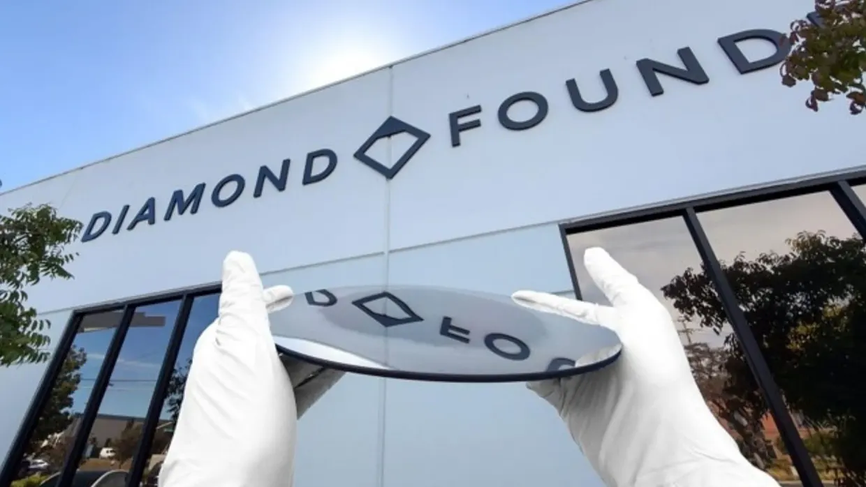
Diamond Foundry announced on November 6 that it has grown a 200-millimeter (7.9-inch) single-crystal diamond in San Francisco, doubling the diameter of its previous 100 mm (3.9 inches) crystal interestingengineering.com
Interesting Engineeringinterestingengineering.comOpen source ↗. According to the company, as reported by Interesting Engineering, the demonstrated prototype represents a single continuous structure rather than a polycrystalline disk. The sample is currently in an unpolished, as-grown state, and its production yield, manufacturing cost, and suitability for commercial chip fabrication remain undisclosed.
Thermal and electrical characteristics
High-purity single-crystal diamond exhibits a thermal conductivity of roughly 2,000 watts per meter-kelvin (W/m·K) at room temperature. This performance exceeds the thermal conductivity of copper and could provide passive cooling solutions for high-performance computing devices and advanced packaging. Furthermore, the material has a wide bandgap of approximately 5.47 electron volts, making it relevant for high-power and high-frequency electronics. However, utilizing diamond as a semiconductor requires addressing integration challenges and doping difficulties to control electrical properties reliably.
Manufacturing steps and scaling
Producing the 200 mm crystal follows 25 years of research by engineers Stefan Gsell and Martin Fischer, according to CEO Martin Roscheisen. The previous 100 mm crystal was grown using diamond heteroepitaxy, although the specific deposition parameters for the 200 mm substrate have not been disclosed. Turning the grown crystal into a commercial semiconductor wafer will require verifying surface flatness, uniform thickness, low defect density, and multi-run repeatability. Diamond Foundry stated that the result makes a future 300 mm (11.8 inches) crystal predictable, alongside plans for a $2.77 billion project in Spain.