Chiba University splits 8×8 mm CVD diamond along the {100} plane with 10 ps laser pulses
In a lab experiment, Chiba University researchers sliced an 8 mm × 8 mm CVD diamond with 10 ps laser pulses. The slice area is about 710 times larger than in their earlier work.
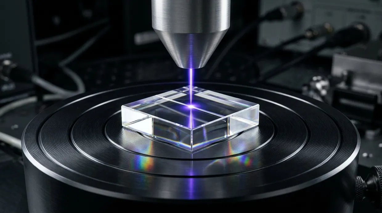
A research team led by Professor Hirofumi Hidai at the Graduate School of Engineering, Chiba University, Japan, has split an 8 mm × 8 mm single-crystal CVD diamond along the {100} plane using ultrashort laser pulses, according to eurekalert.org. The study, coauthored by Mahiro Ikeno, was made available online on September 21, 2026, and published in Volume 169 of Diamond and Related Materials on November 1, 2026 eurekalert.org
eurekalert.orgeurekalert.orgOpen source ↗.
Diamond conducts heat well, has a wide bandgap and is transparent in visible light, which makes it attractive for heat removal, high-power electronics and optics. Its hardness, however, makes it difficult to shape into thin substrates. Laser slicing is being studied as an alternative to mechanical machining: a focused laser creates microscopic modifications inside the crystal, and the resulting internal stresses guide crack propagation. How diamonds made by different methods respond to such treatment was not fully understood.
How different diamonds respond to ultrashort pulses
The team compared three single-crystal diamonds: one made by the high-pressure high-temperature (HPHT) method and two by chemical vapor deposition (CVD), each with a different nitrogen impurity level. The samples were irradiated with pulses from 233 fs to 30 ps. Optical microscopy, spectroscopy and image analysis were used to assess the size, shape and continuity of the modified regions.
The samples responded differently. The two CVD diamonds could be modified with much shorter pulses than the HPHT diamond. In the CVD diamonds, the shortest pulses produced tiny, separated marks, while pulses of about 10 ps or longer produced more continuous modified regions. Nitrogen content alone did not explain the differences, which suggests that microscopic defects tied to each crystal's growth history may matter. CVD diamonds also tended to show less stable modified regions and greater variation in their morphology than HPHT diamonds eurekalert.org
eurekalert.orgeurekalert.orgOpen source ↗.
Slicing along the {100} plane
The researchers then applied 10 ps pulses to an 8 mm × 8 mm CVD diamond, forming modified regions in a controlled grid. Instead of trying to create a full crack network at once, they added modified regions at the midpoints between existing ones. After four such steps, the diamond split cleanly along the {100} plane with a light tap from tweezers. This plane is the easiest to polish.
The slice area was approximately 710 times larger than that of the 300 µm-square HPHT diamond produced in the group's previous study.
Professor Hidai named possible applications as diamond substrates and components for high-power laser optical windows in lithography systems, heat spreaders for advanced electronic devices, and diamond-based power semiconductors. The authors consider the process steps potentially scalable and say the method could be adapted for industrial production of diamond substrates eurekalert.org
eurekalert.orgeurekalert.orgOpen source ↗.