Perovskite/silicon tandem solar cell with a distorted SAM interface reaches certified 35.1% efficiency
Authors report a self-assembled monolayer with tailored intramolecular distortion that coats textured silicon conformally and keeps charge transport, in a lab tandem cell.
A research team reported in Nature a perovskite/silicon tandem solar cell with a certified stabilized power conversion efficiency of 35.1% and a fill factor of 85% doi.org
Naturedoi.orgOpen source ↗. The result was obtained on a laboratory device built on silicon with rough pyramidal textures. The work concerns the design of the self-assembled monolayer (SAM) at the interface between the layers.
The conjugation trade-off in SAM design
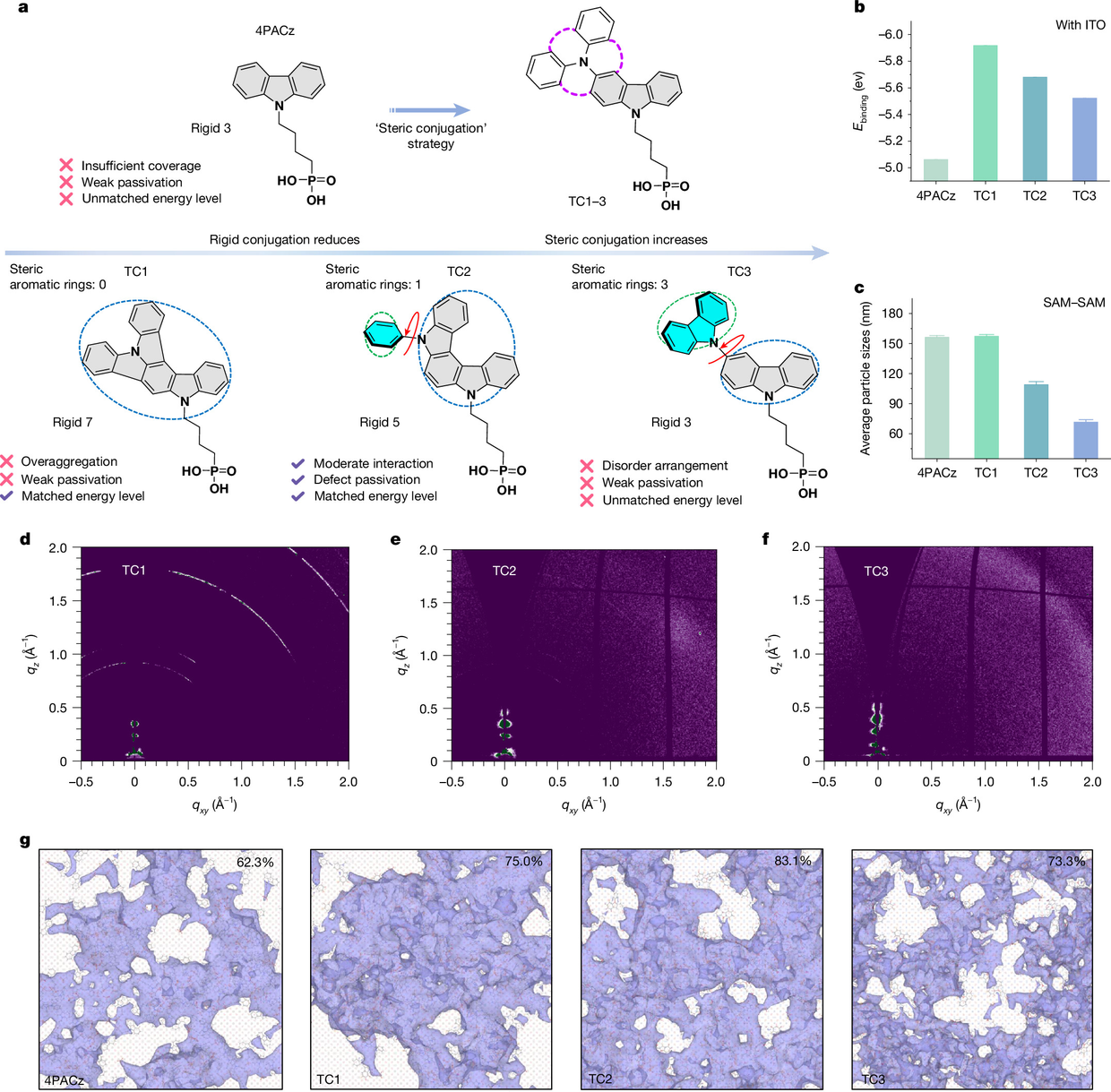
On rough textured substrates, SAM design has been limited by a trade-off. Higher molecular conjugation increases conductivity, but it often leads to unfavourable aggregation that impairs conformal coverage of the surface doi.org
Naturedoi.orgOpen source ↗.
The authors propose a rationally engineered molecular spatial conjugation that includes tailored intramolecular distortion. According to the authors, this suppresses excess π–π stacking without sacrificing charge-transport efficiency doi.org
Naturedoi.orgOpen source ↗. They report that this steric regulation produces a highly ordered, conformal SAM across the rough pyramidal textures
doi.org
Naturedoi.orgOpen source ↗.
Interface function and device performance
The authors state that the resulting interface provides optimized energy-level alignment for ultrafast charge extraction. They also report improved defect passivation through adaptive conformational adjustment of the molecules, and say the layer serves as a template for growth of a high-quality perovskite film doi.org
Naturedoi.orgOpen source ↗.
With this interface, the optimized tandem device reached a fill factor of 85% and a certified stabilized efficiency of 35.1% doi.org
Naturedoi.orgOpen source ↗. In ageing tests under the ISOS-L-1 protocol, the device retained more than 94% of its initial performance after 1,500 hours
doi.org
Naturedoi.orgOpen source ↗.
The authors present the approach as a molecular engineering route to combine conductivity with film uniformity on textured silicon substrates. The reported figures refer to a single optimized laboratory device, not to a commercial module doi.org
Naturedoi.orgOpen source ↗.