University of Stuttgart makes flat silicon UV mirrors from air-hole resonators, focusing 325 nm light
Stuttgart researchers etched elliptical air cavities into silicon to build reflective metasurfaces for 325 nm light. In lab tests the devices focused it to spots of about one micrometer.
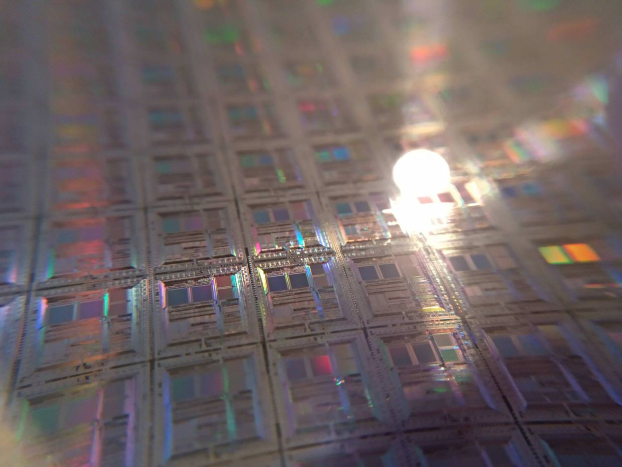
Researchers at the University of Stuttgart have made reflective ultraviolet metasurfaces in silicon that focus light at a wavelength of 325 nm. The work was reported in Advanced Photonics (volume 9, issue 1, article 016002, 2026) and described in a SPIE news release dated 4 November 2026 doi.org
Advanced Photonicsdoi.orgOpen source ↗.
Silicon strongly absorbs ultraviolet light, which rules out the usual approach of solid high-index pillars: light confined inside them would be lost rather than redirected. The authors instead etched small air cavities, called Mie voids, into bulk silicon. Light entering a void reflects from the surrounding silicon boundaries and forms a resonant mode concentrated predominantly in the air, where absorption is negligible doi.org
Advanced Photonicsdoi.orgOpen source ↗.
According to the authors, the strong UV absorption of silicon contributes to this confinement: the optical properties that accompany absorption raise the reflectivity of the air-silicon interface. The method does not remove the absorption, but keeps much of the resonant field away from the absorbing material doi.org
Advanced Photonicsdoi.orgOpen source ↗.
Elliptical voids and focusing
The voids are elliptical, about 470 nanometers long and 100 nanometers deep. Under circularly polarized light, the reflected beam acquires a geometric phase equal to twice the rotation angle of the void. Varying this rotation across a metasurface about half a millimeter in size encodes a focusing profile directly in the silicon. Under an optical microscope the pattern appears as colored rings doi.org
Advanced Photonicsdoi.orgOpen source ↗.
At 45 degrees incidence with 325 nm light, the metasurfaces act as flat equivalents of off-axis parabolic mirrors, turning the beam by 90 degrees while focusing it. Samples with focal lengths from 5 millimeters down to 1.25 millimeters were fabricated and gave circular focal spots as small as about one micrometer. The paper reports numerical apertures up to 0.2, with focal spots approaching the diffraction limit up to a numerical aperture of 0.15 doi.org
Advanced Photonicsdoi.orgOpen source ↗.
Fabrication and beam shaping
The team also added a spiral phase term, up to l=3, to the focusing profile. This is a standard route to beams with orbital angular momentum, which show doughnut-shaped intensity distributions in cross-section doi.org
Advanced Photonicsdoi.orgOpen source ↗.
The metasurfaces are made in a single lithography and etching step on standard silicon substrates, compatible with established semiconductor processing. The authors note that the bulk substrate is mechanically robust and dissipates heat effectively doi.org
Advanced Photonicsdoi.orgOpen source ↗.
They also state that, because the mechanism tolerates and even benefits from absorption, it could be extended to the deep and vacuum UV range and to other material platforms. Since many biomolecules have characteristic UV absorption signatures, the authors suggest such compact elements could eventually be used in integrated sensing doi.org
Advanced Photonicsdoi.orgOpen source ↗.