ECNU laser sub-pulse treatment of amorphous Ga₂O₃ raises UV photodetector responsivity by about 58%
Researchers used programmable sequences of GHz-spaced femtosecond sub-pulses to modify amorphous gallium oxide films with no detectable crystallization. A laboratory UV photodetector improved.
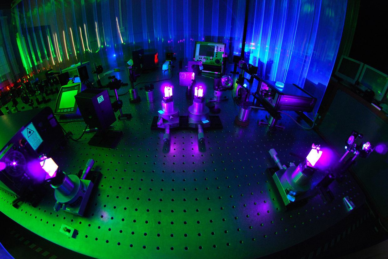
A team led by Heping Zeng at East China Normal University developed a laser method for modifying thin films of amorphous gallium oxide (a-Ga₂O₃) while keeping their predominantly disordered structure. The work, reported in Advanced Photonics, is called digital cold strain engineering (DCSE) doi.org
Advanced Photonicsdoi.orgOpen source ↗. Solar-blind UV photodetectors made from treated films showed responsivity of about 0.126 mA/W against about 0.080 mA/W for untreated ones
doi.org
Advanced Photonicsdoi.orgOpen source ↗.
How the laser sequence works
Strain engineering changes a material's electronic and optical behavior through its structure rather than its composition. In amorphous materials, thermal or mechanical treatment can cause crystallization, cracking or interface damage. DCSE instead uses bursts of femtosecond pulses. The sub-pulses inside each burst are separated at about 1.08 GHz, so the pressure response from one has not relaxed before the next arrives doi.org
Advanced Photonicsdoi.orgOpen source ↗.
The processing condition is set by the integer number of sub-pulses. At constant average laser power, more sub-pulses mean less energy in each, which helps suppress crater-forming ablation. The authors call the process "cold" because energy is deposited faster than it initially diffuses, but they state that it is not entirely free of heat doi.org
Advanced Photonicsdoi.orgOpen source ↗. The team varied the number from 16 to 96, and the trends were not always monotonic
doi.org
Advanced Photonicsdoi.orgOpen source ↗.
Measurements and device results
Grazing-incidence X-ray diffraction showed a broad diffuse pattern with no sharp peaks. Atomic force microscopy found the surface about 0.17 nm smoother and no pronounced craters in the examined regions. Ellipsometry indicated a thickness decrease of about 13.6 nm. The refractive index at 587.3 nm rose from 1.853 to 1.859, and the absorption peak shifted from 263 to 256 nm doi.org
Advanced Photonicsdoi.orgOpen source ↗.
Under 254 nm light at 90 μW/cm² and 1 V bias, the treated device gave a photocurrent of about 12.9 nA against 8.2 nA for the reference, roughly 57% more. Responsivity rose by about 58%, and detectivity by about 25%, from about 4.4×10⁹ to 5.5×10⁹ Jones doi.org
Advanced Photonicsdoi.orgOpen source ↗. Dark current increased moderately, and rise and decay times grew to about 0.5 and 3.2 s from 0.2 and 1.5 s
doi.org
Advanced Photonicsdoi.orgOpen source ↗.
Zeng notes that the pressure simulations are qualitative and do not give the absolute stress in the film. The thickness reduction may involve both structural modification and limited surface-material removal. Scalability and long-term stability have not yet been evaluated doi.org
Advanced Photonicsdoi.orgOpen source ↗.