Mixed-dimensional CMOS of MoS2 and carbon nanotubes: inverters under 1 pW, 19 ps delay
Researchers built laboratory CMOS circuits from single-crystal MoS2 n-type and aligned carbon nanotube p-type transistors, including SRAM and a 4-bit full adder.
Researchers have reported a mixed-dimensional complementary metal–oxide–semiconductor (CMOS) technology that combines two-dimensional single-crystal molybdenum disulfide n-type transistors with one-dimensional aligned carbon nanotube p-type transistors, according to a paper available through doi.org nature.com
doi.orgnature.comOpen source ↗. On this platform the authors fabricated laboratory inverters, static random-access memory (SRAM) and basic logic circuits, up to a 4-bit full adder. These are experimental circuits, not a commercial process.
Complementary integration of nanomaterials
Low-dimensional semiconductors, such as one-dimensional carbon nanotubes and two-dimensional transition metal dichalcogenides, could be used to build scaled, energy-efficient electronic devices. Each material can show excellent unipolar device performance. However, complementary integration with balanced performance and low power consumption remains a challenge, the authors state.
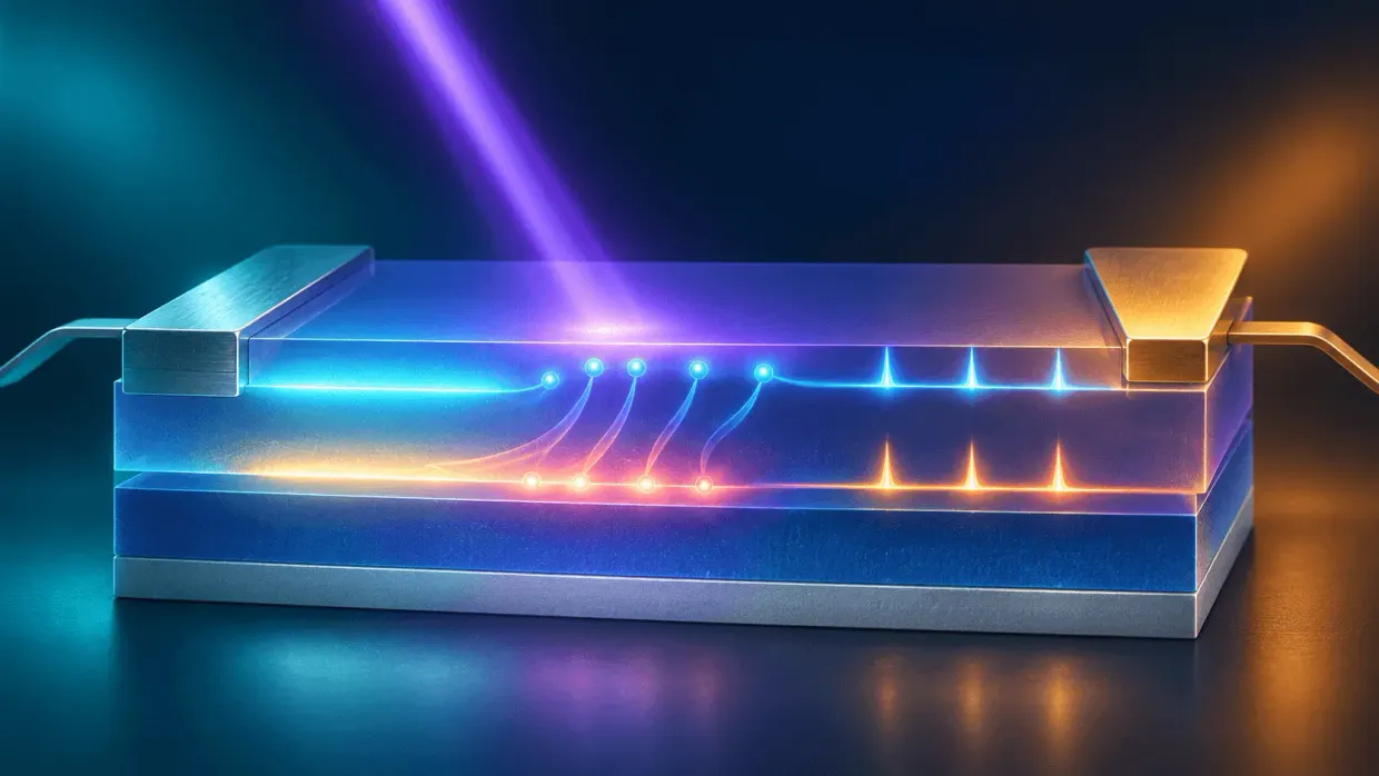
To address this, the team integrated enhancement-mode top-gate transistors with symmetric threshold voltages for both polarities. They achieved this with a hard mask technology and a pre-deposition annealing process. The molybdenum disulfide devices serve as the n-channel and the carbon nanotube devices as the p-channel.
Inverters, memory and logic
The CMOS inverters exhibit rail-to-rail operation, with a peak static power of less than 1 pW and a single-stage delay of 19 ps nature.com
doi.orgnature.comOpen source ↗. The authors also fabricated SRAM at an area equivalent to the 180 nm node. According to the paper, it offers robust read–write operations with a noise margin of 22% and 40% operating voltage.
The uniformity of the transistors and inverters also allowed the authors to create basic logic gates and a 4-bit full adder. Together, these results show that the two material systems can be combined in one complementary circuit platform, from single inverters to arithmetic and memory blocks, at the laboratory stage.