TSMC demonstrates experimental BEOL 1T1C memory with endurance above 100 trillion cycles
The experimental cell has one transistor and one capacitor and sits in the interconnect layers of a processor chip. It may become a more compact alternative to SRAM.
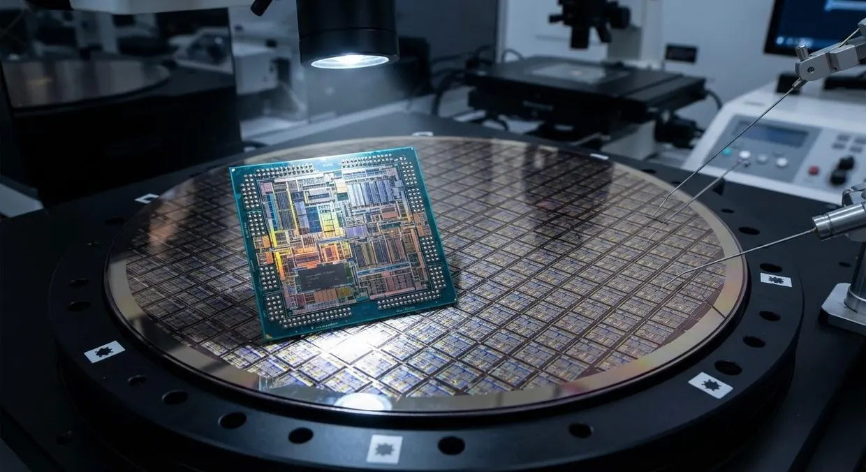
According to ixbt.com, TSMC presented an experimental BEOL (Back-End-Of-Line) memory architecture intended to be placed directly in the interconnect layers of a processor chip ixbt.com
ixbt.comixbt.comOpen source ↗. It is built on 1T1C cells, with one transistor and one capacitor, and may become a more compact alternative to SRAM.
A conventional SRAM cell uses six transistors, so such memory takes up a lot of die area. TSMC's design allows more data to be stored in the same area. The company used an amorphous oxide semiconductor, which gives low leakage currents and allows the memory to be formed without damaging the chip layers.
The experimental sample operated at 0.75 V and retained data for more than 128 ms. A read/write cycle took less than 8 ns, and the stated endurance exceeded 100 trillion cycles.
Earlier reports said TSMC intends to work on 3D DRAM, but the company has not confirmed this. The technology uses vertical cell placement but differs from conventional multilayer DRAM. The timing of commercial adoption is unknown.