Infineon makes functional power devices on 300mm SiC wafers at its Villach fab in Austria
Infineon processed 300mm silicon carbide wafers into working power devices on existing silicon equipment. The larger wafer gives 2.3 times more chips than 200mm.
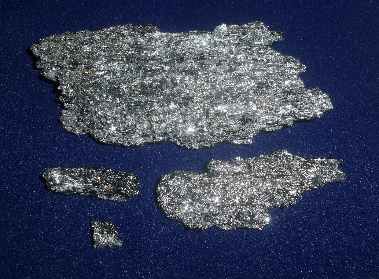
Infineon Technologies AG of Munich, Germany has processed 300mm silicon carbide (SiC) wafers into functional power devices at its fab in Villach, Austria, reports semiconductor-today.com. The company says it is the first to do this in a full-scale semiconductor fab environment. The work used existing silicon manufacturing equipment. semiconductor-today.com
semiconductor-today.comsemiconductor-today.comOpen source ↗
According to Infineon, chip production on 300mm wafers is technologically more advanced and significantly more efficient than on 200mm wafers, since the larger diameter gives 2.3 times more chips per wafer. The company says the result reflects its focus on a comprehensive portfolio of high-performance SiC power semiconductors and on long-term supply. CEO Jochen Hanebeck said that with silicon, gallium nitride and now silicon carbide on 300mm wafers, Infineon is in a leading position to scale semiconductor manufacturing.
Plans for 300mm SiC
Infineon states that the milestone demonstrates the potential of full-scale industrialization of SiC on 300mm wafers. The company will plan the 300mm SiC technology and the ramp timing together with customers and partners, while continuing to execute its 200mm SiC manufacturing roadmap. According to Infineon, advanced SiC power technology gives customers a cost-effective and secure supply base for automotive, renewable energy, industrial and data-center applications.
Cold Split on 300mm SiC
In parallel, Infineon has verified the feasibility of its Cold Split technology with 300mm SiC at its site in Dresden, Germany. Cold Split separates wafers from a SiC boule with less material loss and substantially shorter processing time than conventional wire sawing. More wafers can therefore be obtained from the same crystal with less capital expenditure. semiconductor-today.com
semiconductor-today.comsemiconductor-today.comOpen source ↗
Infineon manufactures semiconductors based on silicon, silicon carbide and gallium nitride. On 27 October it announced an investment of approximately €1.1bn in a high-volume manufacturing facility for GaN power semiconductors on 300mm wafers in Villach. The new SiC result extends this approach to a second wide-bandgap material.
Infineon is showing the processed 300mm SiC wafer in booth 502 (Hall C3) at the electronics trade show in Munich, held 10–13 November.