Columbia extends stroboSCAT microscopy to separate single- and multi-particle transport in semiconductors
Intensity cycling added to transient scattering microscopy isolates single-particle transport in van der Waals semiconductors and tracks exciton–exciton annihilation in lab experiments.
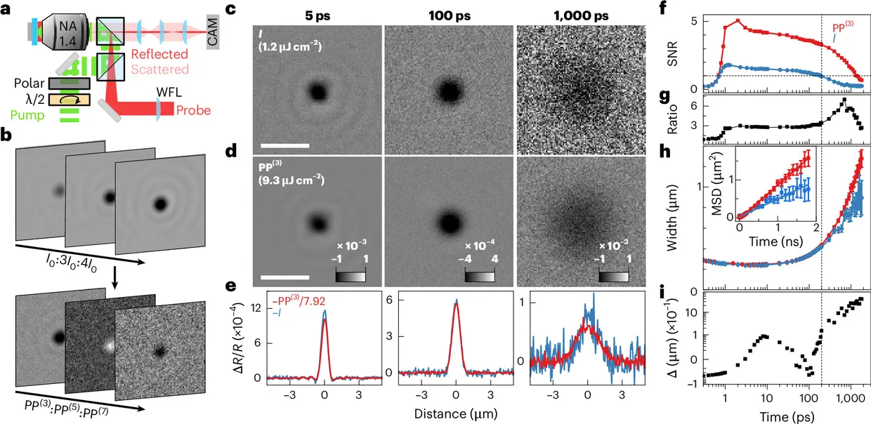
Researchers at Columbia University led by Prof. Milan Delor have extended the stroboSCAT transient scattering microscope with a method called intensity cycling, according to a paper on nature.com. The approach selectively images single-particle and multi-particle transport in van der Waals semiconductors nature.com
nature.comnature.comOpen source ↗. Intensity cycling comes from multidimensional spectroscopy, and here it is applied to the spatiotemporal domain.
Why single- and multi-particle signals overlap
Spatiotemporal optical microscopies image the propagation of electrons, excitons, magnons and polaritons. They provide functional metrics that contact-based transport measurements cannot access. However, they do not distinguish single-particle from multi-particle quantum states, which hinders the study of many-body correlations in materials.
As the researchers describe it, the problem has two sides. At high excitation density, the signals of many simultaneously excited particles overlap. At low density, the signals are often too weak to be separated reliably from noise. StroboSCAT tracks the spread of energy and charge carriers with time-staggered light pulses. The added analysis uses measurements at several excitation strengths and combines the signals of different light intensities computationally. This separates the contributions of single particles from those of two or more interacting particles, while the spatial and temporal information of the microscopy is preserved.
What was imaged
The authors report a series of capabilities demonstrated on van der Waals semiconductors [1]:
- clean isolation of single-particle charge transport with a high signal-to-noise ratio;
- spatiotemporal tracking of exciton–exciton annihilation;
- high-throughput mapping of dielectric disorder;
- imaging of the emergence of a polaronic Mott transition and of correlated transport in a superatomic solid.
The single-particle part of electron transport was resolved in a two-dimensional semiconductor. Such a material consists of extremely thin layers in which mobile charge carriers can influence each other over short distances. Measuring the single-particle contribution separately helps to tell the propagation itself apart from effects of high particle density.
The authors present the result as a precision tool for visualizing how many-body interactions shape material function nature.com
nature.comnature.comOpen source ↗. The work is a laboratory demonstration of a measurement method on specific van der Waals materials.