Hanyang University localizes 2D semiconductor nucleation via oxide etching barriers
Researchers established deterministic single-nucleus growth of molybdenum disulfide, reaching field-effect mobilities of 117 cm² V⁻¹ s⁻¹.
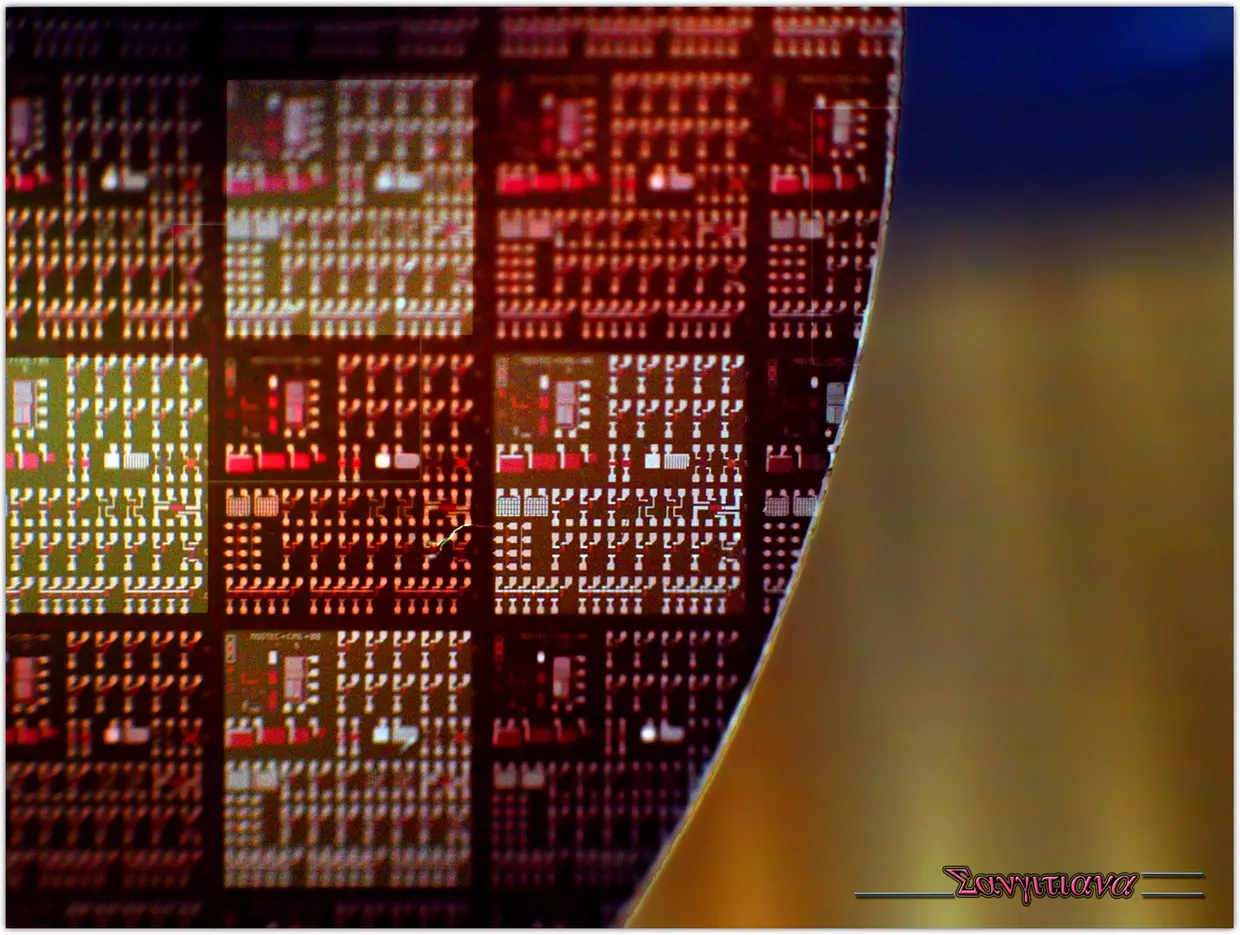
On October 7, 2026, researchers from Hanyang University reported a deposition method termed etching-flux-mediated single-centred nucleation (EF-SCN) in Nature nature.com
Naturenature.comOpen source ↗. The technique localizes individual nucleation events at the center of predefined patterns during metal-organic chemical vapor deposition of two-dimensional semiconductors. The approach suppresses stochastic multi-site crystal formation and yields molybdenum disulfide (MoS₂) single crystals across a 2-centimeter substrate with a single-crystal yield exceeding 99%.
Etching flux mechanism
Conventional area-selective deposition restricts material formation to specific regions but does not control the precise location of nucleation sites within them. In the reported method, growth windows are surrounded by an oxide barrier. When using a hafnium oxide (HfO₂) barrier heated to 750 °C, the material releases oxygen that acts as an in-plane chemical etching flux. This localized flux suppresses embryonic nuclei near pattern boundaries, leaving a solitary stable nucleus at the geometric center that expands outward into a single-crystal domain.
By substituting HfO₂ with zirconium dioxide, which exhibits a lower crystallization temperature, the team reduced the growth temperature to 430 °C while maintaining centrally nucleated triangular MoS₂ domains. Growth regimes were governed by precursor gas ratios: the flow rate of diethyl sulfide determined nucleus density, while the molybdenum precursor flow rate dictated lateral crystal growth boundaries.
Transistor integration metrics
The team produced single-crystal MoS₂ films spanning up to 10-micrometer growth windows with domains approximately 8 micrometers across nature.com
Naturenature.comOpen source ↗. Field-effect transistors fabricated from these domains exhibited carrier mobilities reaching 117 cm² V⁻¹ s⁻¹. Monolithic integration of four transistors within a shared single crystal showed a 7.8% variation in electron mobility, demonstrating line-shaped channel capabilities and self-aligned lateral heterostructures for integrated 2D circuitry.